Showing posts with label PCB. Show all posts

Friday, January 1, 2016

PCB For Polysix OTA Overdrive

Before today, I had made exactly one PCB.  It was a very simple design, yet it was still a painful experience.  I am not an expert -- that's for sure.  Yet, here I'm going to give it another go.  I'm going to dive in and design myself a custom circuit board.  This PCB is going to host my OTA Overdrive Mod for my Korg Polysix.  It'll contain an Arduino-controlled digipot, including my own Arduino as part of the same PCB.  Given my inexperience, this is pretty bold stuff.  I'm nervous and I'm excited.  Can I make it work?

Here's the PCB design that I made using Fritzing.  It's only a two layer board, but it looks awfully complicated for a newbie such as myself.  Does it have any chance of working?

Laying the Groundwork:  Over the last several posts, I've been figuring out most of the elements of this modification, including the digipot and the Arduino.  I know that I want to put all of those elements onto one board and fit it inside my Polysix.  My biggest remaining unknown is how to physically attach my components to the Polysix's circuitry.

Use One of the Built-In DIP Sockets:  A good trick is to re-use one of the DIP sockets that a used throughout the Polysix circuitry.  This is the same trick that I used when installing my mod to add velocity sensitivity to my Polysix.  For this OTA Overdrive Mod, I'm going to use the DIP socket that the OTA itself lives in (ie, IC20 on the KLM-368 "Effects" PCB).

DIP Socket and DIP Connector:  As shown in the picture below, I'm going to pull IC20 out of its DIP socket and I'm going to insert a pinned DIP-style connector in its place.  My PCB will solder to this pinned connector.  To reconnect IC20 into the circuit, my PCB will include its own DIP socket (and associated wiring).  My PCB will include the wiring to connect IC20 back into the Polysix's circuitry via the pinned connector.

I'm going to attach my PCB via the DIP socket for IC20.  It's great that the Polysix came with so many socketed ICs to enable this kind of hack.

Circuit Block Diagram:  Before diving into PCB design, it's important that I understand what it is that I want to do.  The block diagram below shows my overall approach for this PCB.  It shows the DIP connector and DIP socket, it shows the digipot that controls the overdrive, and it shows the Arduino-style microcontroller that controls the digipot.  It also shows the headers that I'll used to program the Arduino ("ICSP" and "FTDI") as well as a bunch of pins and headers that'll let me be flexible in how I choose to connect the various audio and synth control signals that I might wish to manipulate.

Here's a block diagram of what I'm hoping to build.  I want to include lots of pin headers so that I have plenty of flexibility for modifying my own circuit once it's built.

Which PCB Layout Software?  In my previous attempt at a PCB design, I used CadSoft Eagle This is the PCB layout software common throughout the Maker community, probably because there is a free version that is pretty capable.  Both Sparkfun and Adafruit seem to think that it's a good choice for their open source designs.  I didn't like it, though.  I thought that it was hard to learn and didn't promote self-discovery.  I felt like trying a new tool instead.  I almost went for a cloud-based software tool like Autodesk's 123D Circuits, but at the last moment I ended up downloading and trying Fritzing.  I found Fritzing to be very approachable, and unlike 123D Circuits, it's been around long enough for the forums to have a good number of threads for me to learn from.

To layout my PCB, I tried Fritzing.  It seemed much more approachable than CadSoft Eagle.

Parts then Schematic then PCB:  One should only start a PCB design when you already have a good idea about what you want to build.  That's why I started with the block diagram shown earlier and that's why I spent so much time breadboarding the key elements of my circuit in previous posts.  Once you know what elements are going to be in your circuit, only then should you start with the PCB design software.  PCB design software generally follows a three-step process: (1) choose the parts for your design, (2) draw your schematic using your parts, (3) layout your PCB based on your schematic.  OK, here we go...

Step 1A: Choosing my Parts.  Looking back at my block diagram, my major parts are the LM13600 OTA, the AD5262 dual digipot, and the ATMega 328P microcontroller.  For minor parts, there will be a bunch of resistors and capacitors, some pin headers, and an oscillator/clock for the microcontroller.  Fritzing is already well stocked with parts for me to use for these minor components.  So, it's the major components that I need to focus on.  Lucikly, Fritzing already has the version of the ATMega 328P that I want to use (the surface mount TQFP package).  What Fritzing doesn't have is the LM13600 OTA or the AD5262 digipot.  I needed to make these two parts myself.

Step 1B: Creating the Missing Parts.  Making parts is often the hardest part of using PCB design software.  It's such a pain.  I figured it out through a combination of the Fritzing documentation plus lots of trial and error.  The key to making any progress is that Fritzing already had built-in components of the right size.  They weren't the correct part, but they were the correct size (they already had a TSSOP-16 like my digpot and they already had a DIP-16 like my OTA).  As a result, my task was simply to copy the existing parts and re-name the pins.  Through a combination of the built-in part editor (see screenshot below) and a text editor (to change the labels on the SVG graphics), I was able to create my two parts.  If you're interested, I've shared my Fritzing library on my GitHub here.

One of the hardest part of designing one's own PCB is creating models for the parts that don't come in the standard library. Here, I'm making a model for the AD5262 digipot, which is a TSSOP-16 package.  I also did this for the LM13600 OTA, which is a DIP-16.  This process always seems harder than it should be.

Step 2: Create the Schematic.  With my parts created (go me!), I started creating the schematic.  My final schematic is shown below.  In the upper left, you can see a block corresponding to the DIP connector that'll be used to connect this PCB to the Polysix's KLM-368 PCB.  You can see that most of the pins of the DIP connector get routed down to a DIP socket that I'll put on my board to host the LM13600 OTA chip itself.  You can also see that I've broken out few of the LM13600 pins so that I can manipulate the signals (ie, enable overdrive) with the other parts of my circuit.  The rest of the schematic shows the other elements of my circuit -- in particular, you can see the block for the digipot (bottom left) and the big block for the ATMega 328P microcontroller (center).  The critical connections for the 328P (such as the reset circuit) I copied from the Sparkfun Arduino Pro.  That Sparkfun design is also where I learned the layout for the two programming headers (the FTDI and the ICSP headers).

This is the schematic of all the elements that will go into my PCB.  This defines all the connections between the different circuit elements.

Make it Hackable.  As already mentioned, this design breaks out extra Arduino pins, includes some unconnected "spare pins", and includes a second set of pins for both pots in my digipot.  All of these extra access points are to enable future hacking of my own PCB.  I wanted to include flexibility the design of my PCB so that I can make different connections between the OTA, the digipot, and the Arduino.  Who knows what kind of mods I might dream of in the future?!?  With these extra pins, it'll be easier to have fun explorations.  You've got to be prepared to be spontaneous!

Step 3: Layout the PCB.  With the schematic complete, I started the PCB layout process.  I placed my components onto a notional PCB and started laying wires ("traces") between them.  Below is a screenshot showing all of the parts on a notional PCB outline.  I've got about 2/3rds of the traces complete.  To make a trace you simply choose which side of the PCB you want (top or bottom) and then right-click on one of the "air wires" to create the actual trace.  Because the default trace is pretty thick, I would click on the trace and, in the "Inspector" window pane on the bottom right, choose a thinner size like 12 mil.  Finally, click and drag points on the trace to manually route the trace where you want it.  If a trace needs to jump between layers to avoid existing traces, you create a "via" between the layers by right-clicking on the desired spot on the wire.  This is easy!

This is the PCB layout view in Fritzing.  I'm about 2/3rds complete in laying out the board.
Surface Mount vs Through Hole:  I'm not very experienced with surface mount parts (though I have soldered this TSSOP digipot before), so most of my parts in this design are through hole parts (PTH).  The only two surface mount parts (SMT) are the digipot and the ATMega 328P.  In laying out the PCB, the main issue with mixing PTT and SMT parts is that the grid size (which helps keep your traces orderly) really wants to be different for the PTT components vs the SMT components.  For the PTT parts, grid sizes of 0.1", 0.05" or 0.025" all work well.  By contrast, the TQFP package for the ATMega 328P works better with a 0.8 mm (0.0315") grid.  Annoyingly, for the TSSOP package for the digipot, the best grid size is yet a different value (0.0254").  It gets very tedious manually switching between the different grid sizes.

Finishing the PCB:  Once I got all the traces where I wanted them, I started adding text to the PCB so that I could know where to connect my different signals.  I also put a name and date on the board so that I could know which iteration of he board I was using (surely, I would need to iterate the board to fix errors).  Finally, on the bottom layer, I told Fritzing to do a "copper fill".  This is a common technique to try to reduce unwanted noise that may be transmitted between closely spaced circuit boards (such between this PCB and the Polysix KLM-368 that'll be right underneath it).  A screenshot with my final PCB is shown below.  I shared my Fritzing design files on GitHub here.

Still in Fritzing, I have finished my PCB design, including a big copper fill on the bottom for the ground plane.

Design Rule Check:  Throughout the PCB layout process, I would periodically use the software's built-in tool for confirming that my traces were not overlapping with anything else on the board.  The traces on a PCB can get pretty convoluted, so using an automated tool is a great benefit.  This tool is called the "design rule check" (DRC) and is included with almost any PCB design software.  In Fritzing, when I'd run the DRC, I'd get a big pile of error messages like shown in the window below.

The "design rule check" (DRC) gives lots of errors for my design when using the default DRC rules.

Shrinking the Keepout Distance:  When I would try to find these errors in my PCB, I often saw no issue.  The traces (especially around the SMT components) may have been close, but they were not interfering.  I was confused.  The answer is that the default rules used by the DRC algorithm were too tight for my small SMT components.  When I changed the DRC "keepout" distance from its default 0.01" value to a smaller 0.008" value (see screenshot below), almost all of my errors went away.  The remaining DRC errors were legitimate problems, which I found and fixed.

With such small SMT components, you need to reduce the "keepout", thereby telling the DRC algorithms that it is OK if the traces are close together.  I dropped the keepout from 0.01 inches to 0.008 inches.

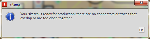
Shrinking the keepout (plus fixing some actual errors in my PCB) eventually lets me pass the DRC.

Export for Production:  Once my design was complete and the DRC results came back clean (see screenshot above...I was so happy when I saw this message!), it's time to export the design so that it can be sent out to be printed.  The exported production files are often called "Gerber Files".  In Fritzing, I chose to export to "Extended Gerber Files".  It created a collection of files that define the top and bottom copper traces, the drill locations for the vias and the PTT components, the top and bottom solder mask, and the top and bottom silkscreen (ie, text and graphics).  These are the files that the printing company need to make the PCB.

Tailor for Your PCB Print Company:  Unfortunately, every PCB printing company is a little different in their requirements for the Gerber files.  As a result, the Gerbers may have to be tweaked specifically for different printing companies.  For me, I chose to use OSH Park to print my board.  Looking at their requirements, the Fritzing Gerber files were all fine, except I had to change my drill file to end with ".xln".  That's all I had to do!  My Gerber files are zipped up on my GitHub here.

Send to Printer:  I uploaded my zipped Gerber files to OSH Park.  Their automated system interprets the files and then shows you illustrations of your design so that you can confirm that they interpreted your files correctly.  In my case, the top and bottom views of my board are shown below.  They look pretty good.


Top and Bottom View of my PCB as Generated by OSH Park.  $21.75 for three.  Let's get it printed!

Order the PCB:  In general, the cost for PCBs is driven by the number of layers (a two-layer board is cheaper than a six-layer board) and by the area of the board (a smaller board is cheaper than a large board).  I tried to make my board pretty small.  I was hoping to get under $20, but I only got it down to $21.75.  Given that OSH Park sends you three copies of your board for that price (plus free shipping!), I'm still pretty happy.  Anyone can order my board from OSH Park here.

Waiting:  So, now I wait for the board to get printed and sent to me.  It generally takes 2-3 weeks.  I'm so excited to get it.  Waiting is agony!

Thursday, August 21, 2014

Testing my MCP4922 PCB

With my custom MCP4922 PCB assembled, it is time to test it.  Soldering is good and fine fun, but the whole point is to get something that actually works!


Connecting to Arduino:  My plan is to connect it to an Arduino and to have it generate a variety of DC voltages.  Unfortunately, it was at this point that I realized I had no female wires to mate to the male headers that I put on my board.  Doh!  So, I had to use alligator clips which are a real pain to work with.  As you can see in the picture above, it is difficult to keep them from touching each other and shorting everything out.

Jumper Some Pins:  Another hiccup is that, as I was hooking it all up to to the Arduino, I realized that I designed my PCB to be overly-general.  Specifically, I when I designed the board, I brought out two of the MCP4922 pins (*SHDN and *LDAC) to the header when I really didn't need to.  For the way that I use this chip, I just need *LDAC tied LOW and *SHDN tied HIGH.  Doing this with alligator clips is annoying, so I just soldered short jumper wires on the bottom of the board to connect these pins to GND and VDD.  This simplified my setup nice.

Arduino Software:  With the hardware all hooked up, I wrote a little Arduino program to drive the DAC.  You can get the code here.  The code outputs two different voltages on the A and B outputs of the DAC to prove that they work.  Output A steps from 0.0V up to 5.0V in one volt increments.  Output B does the opposite -- it steps from 5.0V down to 0.0V in one volt increments.

Victory:  Starting up the program, it automatically stepped through its commands for the different voltages.  I measured the voltages with my digital multi-meter (DMM) to confirm that I was getting the correct output.    As you can see in the pictures below, Output A of the DAC does a pretty good job of hitting the voltages that I wanted.  My first PCB works!  Victory!


Exploring the Error:  Because I'm a nerdy guy, I couldn't leave it there.  I couldn't just enjoy my victory in peace.  No.  I had to look at the results in more detail.  Specifically, I was troubled by the fact that the values reported by the DMM were not quite as close to my desired values as I hoped.

Should be Better?:  I hoped to see exact round numbers spanning 0.0 up to 5.0V.  As you can see in the pictures above, my DMM is reporting values that are off by 1-15 mV.  That seems like a lot of error for a 12-bit DAC.  I mean, on the surface, one might expect an accuracy from the DAC of approximately 1 least significant bit (LSB).  One can compute the magnitude of 1 LSB by scaling from the "full scale" voltage of the device.  Since I'm running it at 5.0V, 1 LSB is (5.0 V / 2^12 bits) = (5.0 / 4096) = 1.2 mV.  This is quite a bit smaller than the 15 mV of error that I'm seeing in some cases.  My gut feeling is that I should be doing better.  So, I started to dig into the details...

Error in Full Scale:  First, note that my DMM shows that the "5.0V" case is actually indicating 5.015V.  This suggests that my "full scale" is actually bigger than 5.0V -- that it is actualy 5.015 V.  In my setup, "full scale" is set by the voltage of the power being delivered to the PCB, which is coming from the Arduino.  The Arduino (Uno) is nominally outputs 5.0V, but it is not a precision voltage reference.  For example, the on-board regulator is only good to +/-50 mV and others have also seen their Arduino "5.0V" be off by 12-14 mV.  So I do not find it surprising that full scale voltage could be running 15 mV higher than expected.  If you want a precise "full scale", you probably have to build/buy a precision voltage reference instead of using the Arduino's 5V pin.

New Expected Values:  What does the 5.015V "full scale" value mean for my expectations for the DAC output?  Well,  since all of the DAC's output values are scaled from this full scale value, the output values that I should actually expect to see are 0.000V, 1.003V, 2.006V, 3.009V, 4.012V, and 5.015V.  These values are closer to the ones that I actually saw, which is good.  My measured values are now only off by 0-6 mV (the worst error is for the 2 V reading).  Still, 6 mV is larger than the 1.2 mV error that I might expect based on 1 LSB, so I'm still not satisfied.

DAC Error from Datasheet:  My next idea is that maybe my expectation of 1 LSB accuracy is wrong.  Digging into the datasheet for the MCP4922, I see in the big table on page 5 under "DC Accuracy" that the INL error can be +/- 4 LSB (!).  If 1 LSB is 1.2 mV, then a 4 LSB error would correspond to 4.8 mV.  That's a lot closer to the 6 mV error that I seem to have...but it's still doesn't account for all of it.

Error in DMM:  My next idea is that maybe the error isn't all with the DAC.  Maybe some of the error is in my DMM.  Looking at the user manual for my Extech EX530 digital multi-meter, it states that the device has an accuracy of "+/- (0.06% reading + 2 digits)".  Let's compute what that means for my problematic 2V reading.  First, at 2V, 0.06% is 1.2 mV.  Second, "2 digits" means 2x the value of the smallest digit on the display.  For the 2V reading, the smallest digit is 0.1 mV, so "2 digits" is an error of 0.2 mV.  As a result, the total error for my DMM could be +/- 1.4 mV.

Total Error:  Combining this 1.4 mV of possible error for the DMM with the 4.8 mV of possible error for the DAC, I get a total error of up to 6 mV. This happens to be the same amount of error that I actually saw.  While that's good (I guess), it is also unsatisfying because it requires all of my errors to be at their maximum.  For now, I'm going to accept that.  But, moving forward, I'm going to keep an eye on how closely my DAC's values are to my desired values.

Thanks for reading!

[Note: The comment section of this post is closed due to too much spam from PCB services.]

Wednesday, August 20, 2014

Assembling my MCP4922 DAC Breakout

One of my most popular posts was this one on making a simple PCB for the MCP4922 DAC.  I'm so glad that people were interested in this!  After a long delay, I have finally decided that it is time to assemble the PCB.  Let's do it!


This post will be mostly pictures showing how I soldered in the parts.  My technique is pretty poor, so don't take this post as guidance on how you *should* do it.  Instead, take this post as comfort that you can be bad at soldering and still get things to work just fine.

First, I got my MCP4922 chip from Digikey.  Currently, $3.14 each, when bought singly.


I inserted the chip into the PCB.  Fits just fine!


I flipped over the PCB to work on the legs of the chip.


I soldered each of the legs:


With all of the legs are soldered, the picture below shows that the joints in the front row are pretty nice, but that the joints in the back row have too much solder.  Oh well.  I'll try to do better next time.


Upon close inspection, I feel that the legs stick out too far.  So, I trim them with my wire snippers.  I wish I had better snippers.  These don't snip very well.  Better ones might let me snip flush against the PCB.


The chip is now fully soldered in place.  The next step is to add the connectors around the edge of the board.  I could have used male pin headers or female.  I only had male headers on hand, so that's what I used.  As you can see below, I used a blank proto-board to hold the pins in place so that they poke up straight through my PCB.  Then I solder them in place.


Once all the pin headers are in place, I need to solder in the two caps (10 uF and 0.1 uF) to decouple the power supply.  In the design of the PCB, I was bold and made both of them be surface mounted parts.  I have barely worked with surface mount components, so I don't really know what I'm doing.  In the picture below, you see me starting by tinning the pads.  I don't know if this is the right thing to do, but here I go...


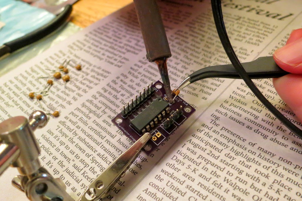
After tinning, I try soldering on the surface-mount capacitor.  I'm not sure what the best technique is.  I had to try it several times until I was able to get both ends of the cap to be decently connected.  I am glad that I bought some nice tweezers, though.


So that was the cap on the bottom of the board.  The other cap is on the top of the board.  Unfortunately, I didn't have another surface mount cap of the right value, so I used a small through-hole cap instead.  I snipped the legs really short and tacked it on with solder.  This is not recommended, but it got the job done.


And, finally, I'm finished! (I left one connector unpopulated because that's just an extra connection for power, which I don't need).


With the assembly complete, the next step is to test it.  That'll be the next post!

Sunday, September 15, 2013

First PCB - Board Has Arrived

As a follow-up to this post, my first PCB has arrived from the printer!  She's a beauty (to my eyes, at least)...and so tiny!


I used my multi-meter to ensure that all the connections go where they are supposed to go, and to confirm that the connections do not go where they are not supposed to go.  It looks like it's time to solder in the components and give it a go!

(Note, this'll also be my first time soldering surface-mount components...I designed the board with one SMT cap on the front and one SMT cap on the, just to give me a reason to give SMT soldering a try.  I'm hopeful!)

Follow-Up: I finally assembled the PCB. Check it out here!

Tuesday, September 3, 2013

First PCB - MCP4922 DAC

I've done it.  I've made the leap.  I've designed my first PCB.  Yay!

Top and Bottom Illustrations of my PCB (from OSH Park)
The purpose of my new PCB is to be a breakout board for the MCP4922 DAC.  This is a 2-channel, 12-bit DAC that I've used for previous projects including: (1) a pitch CV quantizer for my theremin, (2) a pitch CV corrector for my ribbon controller, (3) a CV recorder/looper for my Korg Mono/Poly, and (4) an Arduino wavetable oscillator.  It's this latter project -- the wavetable oscillator -- that I'm looking to resurrect.

I'm eventually looking to make six of these wavetable oscillators -- one for each voice of my Korg Polysix.  On my previous projects, I just wired up each DAC individually by hand on some proto-board.  But, when making six, that's just too full of error possibilities.  So, I designed my first PCB to simplify the construction of six units.  This simple first board will be a stepping stone to my actual goal, which is to build a bigger board that includes two of these DACs (permitting 4 channels of audio and/or CV outputs) along with an Arduino-compatible AVR microcontroller to drive the DACs.  All of this will be on one PCB.  For a guy who has never designed a PCB before, I figured that it would be better to start smaller...such as with this MCP4922 breakout board.

Schematic that I Created in Eagle 6.5
For software to do the PCB design, I chose to use CadSoft Eagle.  I hear that Design Spark might be a better choice (also free, but with fewer constraints than Eagle), but most of the bigger DIY electronics sites (Sparkfun, Adafruit) seem to provide their designs and models in Eagle, so I went with that.

Any PCB design starts with defining the schematic for the circuit that you want to turn into a PCB.  Since I'm just doing a breakout board, the schematic ought to be very simple since their are so few components.  The primary elements are just the IC in the middle and some connectors (or through-hole solder points) around the periphery.  As you can see in the schematic above, I all the input signals to the DAC come in via an 8-pin header on the bottom left (I only needed 7 pins, but the PCB model for the 8-pin looked better).  As for the outputs of the DAC, I brought its two outputs to separate 2-pin headers, as shown on the right side of the schematic.   Pretty straight-forward.

In addition to the connectors around the periphery, it is common for a breakout board to include those supporting components (capacitors and resistors) that are necessary for every likely usage of the chip.  Looking at the chip's datasheet, I see that it always suggests that you use a couple of caps for power supply decoupling, so I included 0.1 uF and 10 uF capacitors in my design.  Also, after looking through the datasheet, I decided that I was never going to want to change the reference voltages applied to the chip, so I just tied those pins to the power supply, which the datasheet said was fine.

The centerpiece of this design is, of course, the MCP4922 chip itself.  Note that labeling on its symbol is poor ("REFDES TYPE", what is that?).  The problem is either that I don't know how to use Eagle (which is true) or that the device model itself is poor because it was robo-translated to Eagle format from the generic format provided by Microchip.  When I was done, I found a model for the MCP4922 in the Adafruit Eagle library.  I should have used that version of the model instead.  But, what's done is done.

2-Layer PCB Design as Performed in Eagle.  Red traces are on the top layer.  Blue are on the bottom.
After completing the schematic, I switched Eagle over to its PCB layout mode.  With a friend's help on how to use the program, I whipped out the design above.  Note that the traces use a few different widths...some are fat and some are skinny.  The inconsistency is my fault and it is only partly by design.  The default trace size is very thin.  I thought it important that the power and ground traces be thicker, especially between the IC and the decoupling caps.  So, I thickened those particular traces by hand.  I did not do a great job.  In the future, I'll try Eagle's "nets" feature so that the trace thickness is more automated.

You'll also note that everything on the PCB is through-hole, except for the two caps, which are SMT (surface mount).  This will be my first time soldering SMT.  Caps are pretty easy, so this should be good training for me.  If it goes well, maybe I'll use more SMT for my future, bigger circuits.

After completing the PCB layout, I had to choose where to get the board manufactured.  Being a fan of Sparkfun, I remembered one of their blog posts that talked about their BatchPCB service being merged with OSH Park.  So, I checked out OSH Park and it looked like a pretty good deal (2-layer board for $5 per square inch, and you get three copies).  A key benefit for me was that OSH Park allows you to upload your Eagle file directly, without going through the error-prone process of exporting Gerber files.  For a newbie like me, that's outstanding.

Before sending my PCB design to OSH Park, I downloaded their DRU file for Eagle, which specifies all of the design limits used in their manufacturing process.  This is important to ensure that your design can actually be fabricated.  When I ran the DRU check on my PCB,Eagle reported some errors with my design.  Mainly it saw that all of my "text" was assigned to the wrong layer.  If I didn't change anything, my "text" was actually going to be printed copper traces on the same layers as the rest of my traces.  This would have shorted everything out!  Oops!  Thank you DRU check!  So, I corrected the problem by moving my text to the correct layer ("21" in Eagle) and re-ran the DRU check.  Now everything was good.

I uploaded my design to OSH Park.  After processing the Eagle file, the OSH Park page produces a bunch of images of my board (like the one at the top of this post) so that I could check the design.  I noticed that some text was written wrong, so I fixed that in my Eagle file and uploaded the design again.  I iterated like this 3 or 4 times before I was happy.  When I was eventually satisfied, I accepted the design.  It's going to be $5.85 for three copies and the shipping is free.  What a deal!

Now I wait for them to arrive.   And to see what design errors I made.  Isn't this hobby fun!?!

(Oh, I shared my PCB design on OSH Park.  If you're curious, you can see it here.)

Follow-Up: The PCB's have arrived!  Check it out here.
Follow-Up: I've assembled the PCB.  Check it out here.
Follow-Up: I've tested the PCB.  It works!  Yay!  Check it out here.

Follow-Up: I've designed my second PCB.  Much more complicated.  You can check out the story here.