 |
| First Generation "Velocity Processor" Installed in my Polysix |
Where to Insert My Circuity: Before I solder anything, I need to figure out where I am going to insert my "Velocity Processor" into the Polysix circuit. As discussed in my previous post, I want to put it after the multiplexer (IC24) but before any of the other envelope and VCF processing. The figure below shows, notionally, how I'll use several of the signals associated with IC24. What is the easiest way to get physically access to these signals?
Use the IC24's Socket! When I opened up my Polysix and too a look at IC24 to see what connection points might be available, I was immediately struck by the fact that IC24 is socketed! By pulling IC24 out of its socket, I now have instant, easy, and easily-reversible access to most of the signals that I need!
 |
| Here is the socket for IC24. The perfect place for inserting my Velocity Processor. |
Which Holes for Which Signals: Looking at the Polysix schematic, I see that I can get almost all of my signals from this one socket: +5V power and ground, the three addressing lines (A,B,C), the inhibit line (INH) as well as a place to inject my velocity-modified, multiplexed envelope signal.
 |
| The signals that I will use for my Velocity Processor -- all available from the socket for IC24. |
How to Connect to the Socket: While the socket is a very convenient way to get signals without modifying the Polysix PCB, I still had to find the right hardware that would mate into the socket. After trying a few options, I found that the legs on the Arduino-style "stackable" headers fit very nicely into the socket. My plan, therefore, would be to mount the stackable headers to a protoboard, solder them in place, and have their legs reach down and mate to the socket. Since these stackable headers have really long legs, they'll let the protoboard (with all of my other components) stand above the other components on the Polysix PCB. It'll be great!
 |
| Arduino-style "stackable" headers fit into the Polysix IC sockets. |
Why Not Use Regular 0.1" Pins? Arduino fans may immediately wonder why I'm using these stackable headers when it appears that 0.1" male pins (also popular with Arduino projects) would be cheaper and less bulky. In fact, I did try to use these pins. But they don't fit in the socket. After looking at the detailed geometry of these pins versus the legs on the stackable header (shown below), I found that the pins are indeed thicker than the legs on the stackable header (0.64 mm vs 0.40 mm). That's the reason that the pins don't fit. That's the reason I'm using these stackable headers. [Note: If you really want to use pins, perhaps the 0.45 mm pins of the Samtech TS-108-T-A will work.]
 |
| The common 0.1" male pins are too thick to fit. But pins the stackable female headers are thin enough to work. |
General Configuration: After looking at the space inside the Polysix, and after looking at the size of the protoboard that I had on-hand, I decided to configure the basic elements of my Velocity Processor as shown below. The stackable headers are shown on the bottom right. The digipot is on the left. The Teensy 3.1 microcontroller is on the top. Now we just need to figure out the wiring.
 |
| Here is my high-level plan: a Teensy 3.1 plus a digipot plus a pair of stackable headers. |
Connections to the Teensy: Below is a picture of the Teensy with the pins labeled. It shows which pins I'm going to use for the various connections. Remember that the Teensy is only a 3.3V device whereas the Polysix's digital signals (the A,B,C addressing lines and the inhibit line) and the Serial connection from my Arduino key Assigner are all 5V signals. Luckily the pins on the Teensy 3.1 are 5V tolerant, so I can attach those lines to the Teensy without damaging it. Another side-effect of the Teensy being 3.3V is that its SPI connections to the digipot will also be 3.3V signals. Therefore, the digipot will have to be provided with a 3.3V reference, which will come from the wire that I show attached to the Teensy's 3.3V supply.
 |
| Connections to my Teensy 3.1 |
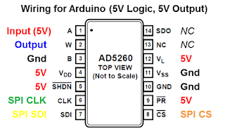
Connections to the Digipot: Below is a figure showing connections that I'm making to the pins of my digipot. As mentioned above, the SPI logic signals are at 3.3V, so I connect the "VL" logic reference (pin 12) as well as to the other logic pins. The multiplexed envelope signal (my "input" to the digipot), however, can span 0V to 5V. Therefore I set VDD to +5V and VSS to ground.
 |
| Connections for the Digipot to handle the 0V-5V Multiplexed Envelope Signal |
The Wiring Plan: The figure below shows my wiring plan for the Teensy, digipot, and IC24 socket. Of course, I still need IC24 itself to function within the circuit. Therefore, I had the brilliant idea to insert another IC socket into the stackable headers! Isn't that brilliant!?! I happened to have a spare IC socket whose legs seemed just long enough to fit in the big holes of the stackable header. So, I can build my velocity processor as shown below, insert the board into the vacated socket for IC24, and then stick IC24 into my board. That's the plan, at least.
 |
| The First Wiring Diagram for my Velocity Processor. Note IC24 sitting on top of the stackable headers in the bottom right. |
The Wiring Reality: Below, you can see the protoboard after I wired and soldered everything in place. You can even see how I inserted IC24 in place. On the underside of the board, you can see the pins sticking out that will fit into the Polysix's socket for IC24.
 |
| The first version of my Velocity Processor |
Testing It: At the top of this blog post is a picture of this first version of my Velocity Processor mounted within my Polysix. While it did do something, I quickly discovered that my plan of sticking IC24 on top of the stackable headers wasn't working. The pins of my add-on IC socket did not mate securely nor reliably to the stackable header. Sad.
The New Wiring Plan: The solution to this problem was to move IC24 off the stackable headers and down onto the protoboard. I had resisted doing this because it mean adding 16 wires (one for each leg of IC24) between the stackable headers and the new spot for IC24. It was going to be an annoying task, but I needed to do it. <Sigh>
 |
| The Second Wiring Diagram for my Velocity Processor. Note that IC24 has been moved and 16 additional wires have been added to connect it to the circuit. |
The Completed Wiring: Below is a picture of my Velocity Processor after moving IC24. You can see it on the top right. You can also see the rainbow of wires that I had to add to connect IC24 back to the stackable headers. All those extra wires sure made it ugly. But, the task is done.
 |
| By moving IC24 to its own spot on the top right, the extra wiring really made it ugly. |
Plugging It In: Below is a picture of my revised Velocity Processor mounted within my Polysix. All of the signals that it needs come up through the IC24 socket into which it has been mounted. The only exception is the serial communication signal that comes from my Arduino Key Assigner. That simplicity is pretty nice.
 |
| My revised "Velocity Processor" installed in my Polysix. |
Next Steps: I need to finish the software on the Velocity Processor and I need to write the companion software for the Arduino Key Assigner so that it conveys the velocity data from the keybed to the Teensy. Then I can test it and make sweet, sweet music. Stay tuned!
Update: It lives! Check out the demo here.


