Friday, October 23, 2015

Velocity Sensitivity - Understanding the Multiplexing

As discussed in my previous post, I have a dream of adding velocity sensitivity to my Korg Polysix.  My replacement keybed already generates the velocity data, I just have to figure out how to use the data.  My plan is to have the velocity affect the intensity of the envelope applied to the filter (VCF).  The harder I hit the key, the more of the envelope signal is applied to the VCF.  Should be easy, right?  Well, it turns out that the Polysix uses a lot of multiplexing to handle its polyphony, including its VCF control.  This post is about understanding the multiplexing so that I can adjust the envelopes based on note velocity.  Let's go!


The Simplified View:  To figure out how the VCF envelope is applied to the VCF, I looked at the Polysix schematic.  Being a six-voice synth, one might expect that six individual circuits are used to apply six individual envelopes to six individual filters.  But this is not the case.  To save money, the designers used multiplexing so that a single circuit could be used to service all six voices.  When I look at the schematic, I do see that there are six circuits used to create the six envelopes.  But then, at IC24, I see that these six envelope signals are multiplexed into a single time-sliced signal.  The single multiplexed signal is then passed through a circuit that combines the envelopes with the VCF cutoff, the VCF key tracking, and the VCF LFO modulation.  At the end of the circuit, IC23 demultiplexes the time-sliced signal back into six individual control voltages that go off to the filter circuit for each voice.

The Detailed View:  With that overview, I have excerpted the real schematic below and highlighted the signal path specific to the VCF envelope.  As can be seen, the six envelope signals enter at the bottom left.  At IC24, they are multiplexed, at which point the time-sliced envelope signal follows the thin red line through the modulation circuit.  Finally, it ends up back at IC23, were it is demultiplexed back into six control signals for each voice's VCF.  Somewhere in this signal path,  we will make a modification to allow us to modify the VCF envelope based on the note velocity.  To decide where and how to make that modification, I need to better understand how the multiplexing works.

Korg Polysix VCF Envelope Processing Circuit, with Annotations

What Does the Multiplexed Signal Look Like?  I hooked up my oscilloscope to the multiplexed signal line shown in the schematic above.  I hit two keys on the keybed and saw what the multiplexed envelope signal looks like.  In the screenshot below, you can clearly see that two envelopes were triggered.  You can also see that the two envelope signals have been sliced up and interleaved.  This is what multiplexing does, it slices up multiple signals and interleaves them onto a single line.  Looks pretty straight-forward, eh?  Let's zoom in, just to be sure of the details.

Voltage at R58.  Two envelopes are multiplexed onto one line.  The second envelope was triggered 6 msec after the first.

Zoomed View:  The picture below is a zoomed in view of the multiplexed envelopes.  As can be seen, there is a repeating signal that contains two two non-zero voltages.  The first voltage value corresponds to the envelope for Voice #1 at a that specific moment in time.  The second voltage corresponds to the envelope for Voice #4 at its moment in time.  In the time between those two voltages, the voltage is zero because none of the other voices are active.  If the other voices were active (as shown later), there would be signal here.  Since the notes are off, there is no envelope, so there is no signal in that time slot.  Easy.  [As a side note, we see that the mutiplexed signal appears to have a cycle of ~310 microseconds, which means that each voice's envelope gets updated at a rate of 3.2 kHz.  I'm actually a bit surprised that it is that slow.  I expected faster.]

Zoomed in view.  Two envelopes on one line.  The second envelope is the Polysix's voice #4 (out of 6).  Note that the pattern repeats every 310 ms, which means that the envelope for each voice is only updated at 3.2 kHz.

All Six Voices Active:  To further illustrate how the envelopes are multiplexed, the screenshot below shows the multiplexed signal when all six voices are active.  In this case, all of the envelopes were triggered at the same time (Unison mode!) so all of the envelopes are showing approximately the same (non-zero) value.  The critical detail here is that we see six period's worth of non-zero signal.  Those are the six voices.  Curiously, we also see two periods of zero signal.  These extra two slots ("slot 7-8") are, in my opinion, purely an artifact of how the addressing is done to keep the multiplexing and demultiplexing in sync with each other.

View at R58 with all six voices active.  Note the empty space, which implies a voice #7 and #8 (which don't exist).

The Vision for Velocity Sensitivity:  Now that I see how the multiplexing works, I can also see how I can modify the envelope signal based on the velocity of each key press.  I think that I can work directly with the multiplexed signal.  In my illustration below, the left portion of the figure is the multiplexed envelope signal as created by the Polysix.  Each color represents the time slice that is associated with each of the six voices.  My idea is that I can introduce a new circuit -- my "Velocity Processor" -- which can attenuate the envelope signal for each voice, depending upon the velocity of the note assigned to that voice.  As long as my Velocity Processor responds fast enough to keep up with the multiplexing, it can affect each voice independently of the others.


Hardware Configuration:  I like this plan -- to simply modify the multiplexed envelope signal based on each notes velocity.  Looking back at the Polysix's hardware, it looks like the right place to introduce my Velocity Processor would be right after the IC24 Multiplexer, as illustrated in the simplified view below.  This location gives me access to the multiplexed envelope signal, but it is before the signal gets too complicated by the rest of the VCF CV processing, where the cutoff, key tracking, and LFO modulations are applied.


Next Step:  The key to this approach is that I want to independently modify each voice in the multiplexed signal stream.  This means that I need to know which voice is on the multiplexed line at each moment in time.  As a result, I really need to dig in and learn about the synchronization and addressing scheme used by the multiplexer.  Figuring this out will be the topic of my next post.

Update:  I figured out the addressing and timing of the multiplexing.  Check it out here.

Update:  I finished the mod.  Behold: Velocity Sensitive Polysix!

Tuesday, October 20, 2015

Velocity Sensitive Polysix - The Dream

As regular readers know, I've done many modifications to my Korg Polysix.  Probably the biggest change was when I swapped out the original keybed for a new one (Fatar, FTW!).  My goal with the new keybed was to add aftertouch to my Polysix, but a side-benefit was that the new keybed was also velocity sensitive.  Unfortunately, the velocity capability has gone unused because the Polysix had no obvious way of including its effect.  Today, though, that begins to change.  Today, I plan out how to add velocity sensitivity to the Polysix.  Behold, the VelocitySix!

Dreaming a Dream of a Dreamy, Velocity-Sensitive, Korg Polysix.  (Fake Graphic)

What Do I Want Velocity to Do?  This is the first question that I asked myself.  What do I want the velocity to affect?  In other synthesizers, the two most traditional answers would be to affect the intensity of the filter (VCF) envelope or of the amplitude (VCA) envelope.  Personally, I've always been a bigger fan of velocity-sensitive VCF, so that's what I decided to target (first, at least).  My idea, therefore, is to add circuitry that will scale the envelope based on the velocity of the keypress.

Scaling the VCF Envelope Based on the Note Velocity

Adding More Hardware:  As can be seen in the figure above, what I need is some hardware that can scale (attenuate) the existing envelope signals.  As discussed in my recent posts, my plan is to do this velocity-dependent attenuation using a digital potentiometer that is driven by a Teensy microcontroller.  I'll simply send the MIDI velocity value for each voice to the Teensy and it will drive the digital potentiometer to adjust the overall amplitude of that voice's VCF envelope.  I'll call the Teensy + digipot my "Velocity Processor".

Piecing it All Together:  The figure below shows all of the components that I've added to my Polysix.  For the addition of velocity sensitivity, I've added my new "Velocity Processor" and highlighted it in yellow.  It is important to realize that I can add this velocity sensitivity only because of my previous modifications.  Without having replaced the built-in keybed with my own keybed and keyscanner, I wouldn't have the velocity values in the first place.  And, without having replaced the built-in "Key Assigner" CPU with my Arduino Mega, I wouldn't know which velocity value to associate with which voice.  It is only through my prior work that this new modification is possible.  [Note: the DAC on the right side of the figure is irrelevant to the velocity sensitivity, but it is crucial for my portamento and detuning modifications.]

My Highly-Modified Polysix.

Building and Testing:  My upcoming posts will discuss the details of how I will manipulate the envelop signals, how I built and tested the new electronics, and how it all sounded when I was done.  This is gonna be fun!


Update:  I've worked out how the Polysix multiplexes its VCF envelopes.

Update:  I've worked out how the Polysix multiplexing handles addressing and synchronization.

Update:  I've wired up the Velocity Processor.

Update:  It works.  It's sweet.  Here are the demos!

Saturday, October 17, 2015

Teensy with AD5260 Digipot

Yesterday, I showed how I soldered a surface-mount digipot, connected it to an Arduino Uno, and got an update rate of just over 60 kHz.  It was pretty fun to get the whole thing working so well.  For my envisioned use of this thing inside my Korg Polsix, however, I need a microcontroller with a little more speed than the Arduino.  It needs to be able to drive the digipot at high speed and do other tasks like listen to messages coming over the serial line.  This post is about using a Teensy to drive the digipot instead.  How fast can it go?

Showing my Teensy 3.1 in the foreground.  It is indeed small.  In the back right is my digipot on its Adafruit SMT-to-DIP adapter board.  An Arduino Uno is in the back left, but it is just being used as a power supply to provide 5V.

What is a Teensy?  Teensy is family of microcontroller boards, like the Arduino is a family of microcontroller boards.  Teensy is aimed at folks who like the Arduino approach but who need something more capable.  In my case, I'm using a Teensy 3.1, which has a 32-bit processor that can run up to 96 MHz.  This is a lot more capability than the 8-bit, 16 MHz processor in the Arduino Uno.  Raw speed, however, isn't my only concern.  The Teensy is appealing to me because you can program it through the Arduino IDE and not have to learn some new way of programming microcontrollers.  Re-using what I know, yet getting more capability.  Sounds like a win-win situation.

Wiring the Digipot for 3.3V Operation:  One somewhat-important difference between an Arduino Uno and a Teensy is that the Teensy operates at 3.3V instead of the Uno's 5V.  This means that the whatever is connected to the Teensy (like my digipot) must be able to respond to the lower voltages.  Lucikly, my digipot is compatible with either 3.3V or 5V logic, so everything should work fine.  The biggest difference is that the output of the digipot (because of the now-smaller 3.3V input signal) will be limited to 0-3.3V, instead of the 0-5V signals seen with the Uno.  For this test, the smaller voltage output is not a problem.  This test is about speed.

Signals to use for testing the digipot with a Teensy 3.1, which uses 3.3V logic.

Wiring to the Teensy:  From the picture above, I'll drive the digipot by providing it power at 3.3V and by sending it commands over via the Teensy's SPI pins.  Looking at the pin map for the Teensy 3.1, I easily see the location of 3.3V and gnd.  Looking for the SPI pins, I see "CS", "SDOUT" and "SCK" on pins 10, 11, and 13, just like on the Arduino Uno!  Maybe that's by design, or maybe it was by coincidence.  Either way, it's comforting to see things being so similar.  So, overall all, as seen below, the wiring is basically the same as it was for the Uno.  Great.

Wiring a Teensy 3.1 to the my digipot via a solderless breadboard.
I connected power (3.3V), ground, and the three lines for the SPI bus.

Teensy Add-On for the Arduino IDE:  With the hardware elements all arranged, it's time to program the Teensy.  Since I want to do this via the Arduino IDE, I needed to first download the "Teensyduino" add-on from the maker of Teensy.  It's pretty painless.  During installation, the installer provides you the option to pre-install a bunch of libraries that Teensy supports.  I chose to install them all, but for this test, you probably just need to install the SPI library.  Either way, it's easy.  Once the Teensyduino software completed its installation, I started the Arduino IDE like normal.  Once it was open, I went under the "Tools" menu (as shown below) and told the Arduino IDE to target the Teensy 3.1 instead of the Arduino Uno.  Done.

I'm switching the Arduino IDE to target my Teensy 3.1 instead of my Arduino Uno.

Programming the Teensy:  With the Teensyduino add-on, my hope was that I could rely on all my Arduino knowledge and not have to learn a new command set just for the Teensy.  Relying on this hope, I simply opened up my existing digipot test program (written for the Arduino Uno) and told the IDE to recompile (Verify" in the language of Arduino).  It was successful!  It recompiled without any changes needed for the Teensy.  Fantastic!  Now, to actually transfer the program down to the Teensy hardware, one has to hit the pushbutton that's on the Teensy board.  When I did that, the program zipped down to the Teensy and I was good to go.  Very smooth.  Very nice.

Driving the Digipot with my Teensy:  With the Teensy programmed and ready-to-go, I hooked up all the wires between my breadboarded digipot and the Teensy according to the figure that I showed earlier.  I then plugged the Teensy into its USB cable (to provide power) and connected my oscilloscope to the output of the digipot.  I saw step-wise changing output voltages, just like I expected.  It worked!

My test setup.  Teensy on the bottom left.  Digipot on a solderless breadboard on the bttom right.  My oscilloscope shows a very quickly changing output signal from the digipot.  It works!

Is it Faster?  How fast could the Teensy change the pot's value?  Very fast.  Very very fast.  As shown in the screenshoot below, it was able to change the value six times in 8.1 microseconds (usec).  That's a mere 1.35 usec per change.  That's an update rate of 741 kHz!  By comparison the Uno required 16 usec, which was an update rate of 62.5 kHz.  So, the Teensy was about 12 times faster for this task.  That's fantastic.  Interestingly, the ratio of the their clock speeds (Teensy = 96 MHz, Uno = 16 MHz) is only 6x, so by actually showing a 12x increase in speed, it appears that the Teensy is much more efficient per clock cycle at this task than the Arduino.  Very cool.

[Note: Based on questions I've received...yes, I did disable the println() and delay() commands when testing at full speed.  I love that you folks are reading in this kind of detail! :) ]

Screenshot of the output of the digipot when being driven at full speed by the Teensy.  Note that it completes a six step cycle in 8.1 usec, which means that each step is only 1.35 usec, which means that the Teensy can drive the digipot with an update rate of 741 kHz.  Fast!

Extra Capacity for Other Tasks:  If I use this Teensy+Digipot setup in my nefarious plans for my Korg Polysix, I do not need it to update this fast.  At worst, I'll need it to update every 20 usec, which means that the Teensy can do its update at its native 1.35 usec speed and then wait around for the other 18.65 usec and do other tasks.  In other words, it'll only be busy (1.35/20) = 7% of the time.  The other 93% of the time, it'll be free to do things like servicing in-coming Serial messages.  I like having that much margin.  It gives me confidence that the Teensy can perform all of its tasks dependably.  My conclusion is that I've found my winning hardware combination for my Polysix modifications.

Friday, October 16, 2015

Surface Mount DigiPot with an Arduino Uno

For an upcoming modification to my Korg Polysix, I need to be able to attenuate an analog signal in response to the user's inputs.  This is a perfect task for a a digital potentiometer.  If I can, I'd like to control the digipot from an Arduino, because an Arduino is so easy to program.  There are two challenges with this plan, however.  First, my preferred digipot is only available as a surface mount device.  Second, I'm worried that the Arduino is too slow to drive the digipot quickly.  Well, I do like challenges, so let's just dive in and see where we can get!

Driving my digipot with an Arduino Uno.  How fast can it go?


Choosing my Digipot:  There are many digital potentiometers on the market.  For use inside my Polysix, I might need to put digipot in a place where it would need to control voltages ranging from -5V to +5V.  Most digipots cannot handle this kind of bipolar voltage range (most are just 0-5V).  Of the choices that I saw on Digikey for bipolar digipots, I chose to buy an Analog Devices AD5260 (link).  As you can see it in the picture below, it's a tiny little surface-mount device.  Scary!  (actually, don't be scared...it'll be fine)

Analog Devices AD5260 Digital Potentiometer.  Surface Mount!  Tiny!

Surface-Mount Adapter Board:  Because I'm usually just hacking stuff together, and because through-hole components are much easier to hack with, I don't have nearly zero experience soldering surface-mount components.  If I made my own circuit boards, I would certainly use more surface mount components because they save so much space.  For this hack, however, I need flexibility to plug, unplug, and reconfigure my circuit.  Therefore, I'm going to put my surface mount device onto a an adapter board that gives it legs like a through-hole component.  My digipot is a TSSOP-14 package, so I bought a TSSOP-14 adapter board from Adafruit.  It comes as a pack of 6, so I have spares in case I make a mistake.  :)

Mounting my surface-mount digipot to a through-hole adapter board.

Soldering Surface Mount ICs:  How do I actually do the soldering?  I talked with a co-worker who is extremely experienced in this area and he gave me a pile of good advice.  Two parts of that advice were: (1) use very fine (thin) solder and (2) use lots of flux.  Unfortunately, by the time I got around to soldering (days later), I had forgotten these two important details.  As a result, using my too-thick solder and using no extra flux, I created many solder bridges between the tiny legs of this tiny IC.  This is not what you want to do.  But, through perseverance, and through extensive use of solder wick to remove excess solder, I finally got the IC soldered no shorts or bridges.

Magnification (Or, How to Look Cool):  One piece of my colleague's advice that I did follow was to use some magnification.  He let me borrow an "OptiVisor" (see picture below).  It doesn't feel like it provides much magnification, but it is enough to give a clear view.  And, I'm learning that if you can *see* it, you can solder it.  The OptiVisor provides that.  They're also quite fashionable (that would be sarcasm).  

It definitely helps to use some magnification so that you can see what you're soldering.

Add Legs for Breadboarding:  The Adafruit adapter board has through-holes on either side for attaching pin headers.  As you can see below, I used a regular piece of 0.1" break-away pin header.  I broke off two seven-pin segments, temporarily placed them into my solderless breadboard, put the digipot board on top, and soldered the pins on.  This through-hole stuff is easy!

Soldering the pins to the breakout board so that I can easily prototype with the digipot.
Using a solderless breadboard keeps everything aligned while you solder.

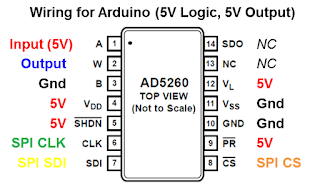
Deciding How to Connect:  With the digipot's adapter board finished, I had to figure out how to wire up the device.  Below is a picture from the digipot's datasheet with my own labels added to show what I would connect to each pin.  All connections were going to my Arduino.  As you can see, there are a bunch of 5V and Gnd connections.  Commands are sent via the SPI bus, so there are also the three SPI connections (theSDO line is not needed as there is no communication needed back to the Arduino).  Finally, for the pot's input, I'll simply apply 5V, which means that my output will be a DC voltage that is scaled between 0-5V.

Signals to use for testing the digipot with an Arduino, which uses 5V logic.

Wiring to the Arduino:  The wiring plan shown above requires 12 connections.  Since I am usually prone to error when doing my wiring, I choose to draw up a little picture to fully illustrate to myself how I should use my solderless breadboard to make all of these connections.  This extra "design" effort really made the wiring process much easier.  It also made the wiring process more reliable.  Once I got the Arduino software working, the wiring of the hardware worked on the first try!

Wiring an Arduino Uno to the my digipot via a solderless breadboard.

Writing the Arduino Software:  To change the value of the digipot, I had to write some Arduino code to send commands to the digipot via the Arduino's SPI pins.  I started with the Arduino's built-in example called "DigitalPotControl".  While that code is simple and easy to understand, I wasn't sure if it runs the SPI bus as the fastest possible setting.  Speed is critical for using this in my Polysix, so this detail was worth a little effort.  After Googling around, I found the correct Arduino commands to control the SPI bus speed and I wrote my test program (SPI mode is zero!).  My program is shared on my GitHub here.

Initial Test:  My test program steps through a range of the digipot values.  It stops at each step for three seconds, which gives me enough time to confirm that its output is correct.  Because the input of my digipot is connected to +5V, my output will be between 0V and 5V.  For the picture below, the digipot was at a value of 125 (out of 255), which resulted in an output voltage being 2.47V.  Given that I expected (125/255*5) = 2.45V, I got pretty decent agreement.  In other words, it works!

First test.  It successfully created a voltage half-way between 0-5V. 

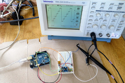
Testing for Speed:  Now for the full speed test.  I commented out the delay() and println() commands and restarted the system.  If used in my Polysix, there will only be 15-20 microseconds (usec) to change value of the digipot.  This means that the Arduino + digipot must support an update rate of 50-67 kHz, which seems pretty fast for an Arduino.  To see how fast my system was actually running, I connected the output of the digipot to an oscilloscope.  The full setup is shown at the picture at the top of this post.  A screenshot from the oscilloscope is shown below.

The Uno is changing the digipot as fast as it can.  It takes 16 usec per step, which results in an update rate of 62.5 kHz.

How Fast is It?  The picture above shows that the digipot is only being updated every 16 usec, which means it has an update rate of 62.5 kHz.  This is within my 50-67 kHz requirement.  So that's good, right?  Well, no, not exactly.  I am a little uncomfortable with the fact that there is no margin.

The Need for Margin:  In achieving this 62.5 kHz result, the Arduino is doing nothing but updating the value of the pot over and over endlessly.  That is all that the Arduino is doing.  In my envisioned hack for Polysix, however, my Arduino would need to do a few other tasks, as well.  For example, the Arduino will need to listen to its Serial port so that it can receive commands as to what values to use for the pot.  If the Arduino is running flat-out just to maintain a high update rate, it probably wouldn't have enough spare cycles to service the serial port.  That would be unacceptable.  So, while it is exciting that I got the system to operate this well, I think that the that the Arduino Uno isn't quite fast enough.  I need to try something else

Trying a Teensy:  My next step is to try a faster Arduino.  Or, an even better plan would be to step up to the fastest Arduino-like board that I know: Teensy 3.  But I think that'll have to wait until my next post.

Update:  My results with the Teensy are here.  The Teensy is *really* fast!

Sunday, April 26, 2015

S-Triggers from TR-707 Drum Machine

I have a Roland TR-707 drum machine and I have a couple of pre-MIDI Korg synths (a Mono/Poly and a Polysix).  Since there's nothing more fun than sweet acid-like basslines combined with propulsive trance-inducing drum beats, it's crucial that my old synths be able to synchronize to the drum machine.  This post is about modifying my 707 to finally make it control my synths the way that they should be controlled -- my 707 now outputs S-Trigs!  First, here's a demo...


Previous Attempts

TR-707 Trigger Out:  The 707 does have an output ("Trigger Out") whose purpose is to synchronize to external gear, such as the arpeggiators in these old synths.  As shown in a previous post, however, the built-in Trigger Out doesn't work for driving the Mono/Poly.  It does work with the Polysix, but it is late by 40 msec due to the V-Trig vs S-Trig issue (as discussed later).  So, in the end, the built-in Trigger Out doesn't work for my old synths.

Arduino MIDI-to-Trigger Converter:  Since the stock 707 Trig Out doesn't work, I hacked together my own MIDI-to-Trigger converter. This Arduino-based device listens to the MIDI clock output by any device (such as from the TR-707) and generates properly synchronized trigger pulses to drive my synths (two arpeggiators at once is fun!).  The problem, though, is that I don't like all the clutter of the extra wiring associated with this setup.  It's not ideal.

Modifying the 707 for S-Trig

V-Trig vs S-Trig:  Why doesn't the 707's built-in Trig Out work?  The problem is that 707 outputs "V-Trig", whereas my old Korgs expect "S-Trig".  What?  A V-Trig is a signal that is normally low (0V), which then pulses high (5V) for each trigger.  Unfortunately, my two old Korg synths expect an "S-Trig", which is the opposite -- a normally high signal that then shorts to ground for each trigger.  This difference between V-Trig and S-Trig means that my 707 doesn't play well with my Korg synths.

The 707 is Actually S-Trig Internally:  After looking through all the schematics, I noticed that inside  the 707, the circuitry actually utilizes S-Trig to trigger its internal drum sounds.  The only V-Trig signal generated by the 707 is the Trig Out provided to the user.  As shown in the schematic excerpt below, even this signal actually starts as an S-Trig that is then inverted into V-Trig by Q13.  So, given that all of these S-Trig signals are already inside the 707, I decided to modify the 707 so that it could output its S-Trig signals.

The TR-707 Trigger Out is "V-Trig", but internally it is "S-Trig"

The Simplest Plan:  Looking at the schematic above, one easy way to output S-Trig would have been to simply take the S-Trig from CPU pin 21 and wire it directly to the output jack.  But, this would have had two problems: (1) these old CPU chips are generally too fragile to be in direct electrical contact with the outside world, and (2) I would have lost the existing V-Trig output, which I might want to use with other gear in the future.  I need a better plan.

A Better Plan:  My better plan is to find a more robust source for S-Trig signals (ie, anything but the CPU) and to output the signal using other jacks on the back of the 707 (so that I keep the built-in Trig Out).  Which jacks?  Well, I never use the cassette tape interface, so I'll re-use those two jacks to give myself *two* S-Trig outputs.  Exciting!

Here's the back of the TR-707.  I'm not going to replace the built-in V-Trig.
Instead, I'll mod the 707 to output S-Trig on these two jacks that I never use.


Re-Wiring the Jacks

Where to Connect:  To use these two jacks, I need to disconnect the jacks from the existing circuit.  Looking at the schematic (excerpt below), the easiest solution would be to remove the resistor R51 for one of the jacks and to remove C30 for the other jack.  While this would work, it's usually a good idea to always have a series resistor in line with an output jack in case someone (ie, me) plugs in something stupid by accident.  The in-line resistor helps limit any currents that could damage the circuitry.  So, to leave a resistor in-line, I chose to pull the right leg of R51 and to pull the right leg of R43.   That disconnects the other circuitry while leaving the resistors in-place for me to re-use later.  It also leaves in-place the capacitor (C30), which I don't want, but which I can deal with later.

I can disconnect the two jacks from the existing circuit by de-soldering the legs of these two resistors.
Smell the Solder:  To disconnect the targeted leg of each resistor, I applied my soldering iron to the back side of the circuit board (PCB) and used small-nosed pliers to wiggle/pull on the resistor leg until it came free.  You can see each resistor's free leg in the photos below.  Later, I'm going to solder a new wire to the free leg, so make sure that the legs are still accessible.

De-soldering one leg of each resistor.  Make sure you de-solder the correct leg!

Getting the S-Trig Signals

Find a Source:  After preparing the output jacks, my next step was to find a good source for S-Trig signals.  Looking at the 707's schematic (see excerpt below), I see that the internal drum sounds are triggered by IC28 (a TC40H174P, which is a basic CMOS flip-flop).  This looks like a great place to get our S-Trig signals because, if IC28 were to get damaged as a result of this mod, this chip is much easier to replace than the CPU itself.  [Note that TC40H174P is no longer available, but a 74LS174 seems to do the same thing].  Let's get our S-Trig signals here.

Get the S-Trig from IC28, because that 40H174 is easy to replace if I damage it.

Soldering in the Wire:  To actually get this signal out, I could solder a wire directly to IC28, but my poor soldering skills mean that I risk damaging the IC by overheating it.  Instead, I'm going to solder my wire to R83, because resistors are very hard to damage.  You can see my soldered result below -- the red wire goes to R83 to get the trigger for the "Rim/Cowbell" sound.  For my second S-Trig, I chose to grab the trigger signal for the "High Tom" (the yellow wire, connecting via R87), but you can choose whichever sound you'd like.

Soldering wires to get the S-Trig signals that I want.

Connecting Back to the Jacks

The Connection Plan:  Now that I have the S-Trig signals on the red and yellow wires, I soldered those wires to the free legs of R51 and R43 (see schematic below).  These are the two resistors that I partially de-soldered from the circuit board to disconnect the jacks from the rest of the circuit.  By soldering to the free leg of each resistor, I've now connected the jacks back to the S-Trig signals produced by IC28.

Connecting the output jacks to the S-Trig signals from R83 and R87.

Jumper C30:  The last modification is to remove the effect of C30 (see schematic above) because it will interfere with the S-Trig signal that I'm trying to output.  The easiest way to "remove" it is to simply solder a jumper wire across its two terminals.  You can see the little jumper that I added in the picture below.  Easy.

I added a jumper wire across C30 to remove it from the circuit.  Otherwise,
it could interfere with outputting the S-Trig signal.

Tuck in the Wires:  The picture below shows my final wiring.  The red wire is connecting the "Rim/Cowbell" trigger from its source on the bottom-right up to the output jack on the top-left.  The yellow wire connects the "High Tom" trigger from the bottom-right up to the top-left.  I tucked in the wires between the components to ease my re-assembly of the drum machine.

The final wiring of the "Rim" and "High Tom" triggers from their source on
bottom-right up to the output jacks on the top-left.

Put It Back Together

With the wiring complete, I re-assembled the drum machine and tested it out.  I confirmed that the built-in "Trig Out" still works (using my Micro Brute, which accepts V-Trig) and I confirmed that my two new S-Trig outputs work (using my Mono/Poly).  You can see my test of the S-Trig outputs in the video at the top.  Hacking success!

I re-used the "Tape Out" and "Tape In" jacks as outputs for S-Trig signals.
The left jack is activated on the "Rim/Cow" triggers.
The right jack is activated on the "High Tom" triggers.


Thursday, August 21, 2014

Testing my MCP4922 PCB

With my custom MCP4922 PCB assembled, it is time to test it.  Soldering is good and fine fun, but the whole point is to get something that actually works!


Connecting to Arduino:  My plan is to connect it to an Arduino and to have it generate a variety of DC voltages.  Unfortunately, it was at this point that I realized I had no female wires to mate to the male headers that I put on my board.  Doh!  So, I had to use alligator clips which are a real pain to work with.  As you can see in the picture above, it is difficult to keep them from touching each other and shorting everything out.

Jumper Some Pins:  Another hiccup is that, as I was hooking it all up to to the Arduino, I realized that I designed my PCB to be overly-general.  Specifically, I when I designed the board, I brought out two of the MCP4922 pins (*SHDN and *LDAC) to the header when I really didn't need to.  For the way that I use this chip, I just need *LDAC tied LOW and *SHDN tied HIGH.  Doing this with alligator clips is annoying, so I just soldered short jumper wires on the bottom of the board to connect these pins to GND and VDD.  This simplified my setup nice.

Arduino Software:  With the hardware all hooked up, I wrote a little Arduino program to drive the DAC.  You can get the code here.  The code outputs two different voltages on the A and B outputs of the DAC to prove that they work.  Output A steps from 0.0V up to 5.0V in one volt increments.  Output B does the opposite -- it steps from 5.0V down to 0.0V in one volt increments.

Victory:  Starting up the program, it automatically stepped through its commands for the different voltages.  I measured the voltages with my digital multi-meter (DMM) to confirm that I was getting the correct output.    As you can see in the pictures below, Output A of the DAC does a pretty good job of hitting the voltages that I wanted.  My first PCB works!  Victory!


Exploring the Error:  Because I'm a nerdy guy, I couldn't leave it there.  I couldn't just enjoy my victory in peace.  No.  I had to look at the results in more detail.  Specifically, I was troubled by the fact that the values reported by the DMM were not quite as close to my desired values as I hoped.

Should be Better?:  I hoped to see exact round numbers spanning 0.0 up to 5.0V.  As you can see in the pictures above, my DMM is reporting values that are off by 1-15 mV.  That seems like a lot of error for a 12-bit DAC.  I mean, on the surface, one might expect an accuracy from the DAC of approximately 1 least significant bit (LSB).  One can compute the magnitude of 1 LSB by scaling from the "full scale" voltage of the device.  Since I'm running it at 5.0V, 1 LSB is (5.0 V / 2^12 bits) = (5.0 / 4096) = 1.2 mV.  This is quite a bit smaller than the 15 mV of error that I'm seeing in some cases.  My gut feeling is that I should be doing better.  So, I started to dig into the details...

Error in Full Scale:  First, note that my DMM shows that the "5.0V" case is actually indicating 5.015V.  This suggests that my "full scale" is actually bigger than 5.0V -- that it is actualy 5.015 V.  In my setup, "full scale" is set by the voltage of the power being delivered to the PCB, which is coming from the Arduino.  The Arduino (Uno) is nominally outputs 5.0V, but it is not a precision voltage reference.  For example, the on-board regulator is only good to +/-50 mV and others have also seen their Arduino "5.0V" be off by 12-14 mV.  So I do not find it surprising that full scale voltage could be running 15 mV higher than expected.  If you want a precise "full scale", you probably have to build/buy a precision voltage reference instead of using the Arduino's 5V pin.

New Expected Values:  What does the 5.015V "full scale" value mean for my expectations for the DAC output?  Well,  since all of the DAC's output values are scaled from this full scale value, the output values that I should actually expect to see are 0.000V, 1.003V, 2.006V, 3.009V, 4.012V, and 5.015V.  These values are closer to the ones that I actually saw, which is good.  My measured values are now only off by 0-6 mV (the worst error is for the 2 V reading).  Still, 6 mV is larger than the 1.2 mV error that I might expect based on 1 LSB, so I'm still not satisfied.

DAC Error from Datasheet:  My next idea is that maybe my expectation of 1 LSB accuracy is wrong.  Digging into the datasheet for the MCP4922, I see in the big table on page 5 under "DC Accuracy" that the INL error can be +/- 4 LSB (!).  If 1 LSB is 1.2 mV, then a 4 LSB error would correspond to 4.8 mV.  That's a lot closer to the 6 mV error that I seem to have...but it's still doesn't account for all of it.

Error in DMM:  My next idea is that maybe the error isn't all with the DAC.  Maybe some of the error is in my DMM.  Looking at the user manual for my Extech EX530 digital multi-meter, it states that the device has an accuracy of "+/- (0.06% reading + 2 digits)".  Let's compute what that means for my problematic 2V reading.  First, at 2V, 0.06% is 1.2 mV.  Second, "2 digits" means 2x the value of the smallest digit on the display.  For the 2V reading, the smallest digit is 0.1 mV, so "2 digits" is an error of 0.2 mV.  As a result, the total error for my DMM could be +/- 1.4 mV.

Total Error:  Combining this 1.4 mV of possible error for the DMM with the 4.8 mV of possible error for the DAC, I get a total error of up to 6 mV. This happens to be the same amount of error that I actually saw.  While that's good (I guess), it is also unsatisfying because it requires all of my errors to be at their maximum.  For now, I'm going to accept that.  But, moving forward, I'm going to keep an eye on how closely my DAC's values are to my desired values.

Thanks for reading!

[Note: The comment section of this post is closed due to too much spam from PCB services.]

Wednesday, August 20, 2014

Assembling my MCP4922 DAC Breakout

One of my most popular posts was this one on making a simple PCB for the MCP4922 DAC.  I'm so glad that people were interested in this!  After a long delay, I have finally decided that it is time to assemble the PCB.  Let's do it!


This post will be mostly pictures showing how I soldered in the parts.  My technique is pretty poor, so don't take this post as guidance on how you *should* do it.  Instead, take this post as comfort that you can be bad at soldering and still get things to work just fine.

First, I got my MCP4922 chip from Digikey.  Currently, $3.14 each, when bought singly.


I inserted the chip into the PCB.  Fits just fine!


I flipped over the PCB to work on the legs of the chip.


I soldered each of the legs:


With all of the legs are soldered, the picture below shows that the joints in the front row are pretty nice, but that the joints in the back row have too much solder.  Oh well.  I'll try to do better next time.


Upon close inspection, I feel that the legs stick out too far.  So, I trim them with my wire snippers.  I wish I had better snippers.  These don't snip very well.  Better ones might let me snip flush against the PCB.


The chip is now fully soldered in place.  The next step is to add the connectors around the edge of the board.  I could have used male pin headers or female.  I only had male headers on hand, so that's what I used.  As you can see below, I used a blank proto-board to hold the pins in place so that they poke up straight through my PCB.  Then I solder them in place.


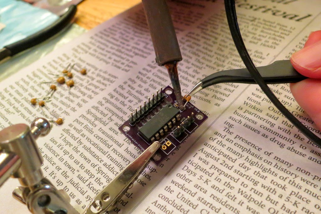
Once all the pin headers are in place, I need to solder in the two caps (10 uF and 0.1 uF) to decouple the power supply.  In the design of the PCB, I was bold and made both of them be surface mounted parts.  I have barely worked with surface mount components, so I don't really know what I'm doing.  In the picture below, you see me starting by tinning the pads.  I don't know if this is the right thing to do, but here I go...


After tinning, I try soldering on the surface-mount capacitor.  I'm not sure what the best technique is.  I had to try it several times until I was able to get both ends of the cap to be decently connected.  I am glad that I bought some nice tweezers, though.


So that was the cap on the bottom of the board.  The other cap is on the top of the board.  Unfortunately, I didn't have another surface mount cap of the right value, so I used a small through-hole cap instead.  I snipped the legs really short and tacked it on with solder.  This is not recommended, but it got the job done.


And, finally, I'm finished! (I left one connector unpopulated because that's just an extra connection for power, which I don't need).


With the assembly complete, the next step is to test it.  That'll be the next post!